- 您现在的位置:买卖IC网 > Sheet目录366 > TMDXEVM5515 (Texas Instruments)EVAL MODULE DSP FOR C55XX
SPRS645F – AUGUST 2010 – REVISED OCTOBER 2013
5.5.3
Clock PLL Electrical Data/Timing (Input and Output Clocks)
Table 5-4. Timing Requirements for CLKIN (1)
(2)
NO.
CV DD = 1.05 V
MIN NOM
MAX
MIN
CV DD = 1.3 V
NOM
MAX
UNIT
88.577,
88.577,
1
t c(CLKIN)
Cycle time, external clock driven on
CLKIN
83.333,
or
83.333,
or
ns
81.380
81.380
2
3
t w(CLKINH) Pulse width, CLKIN high
t w(CLKINL) Pulse width, CLKIN low
0.466 *
t c(CLKIN)
0.466 *
t c(CLKIN)
0.466 *
t c(CLKIN)
0.466 *
t c(CLKIN)
ns
ns
4
t t(CLKIN)
Transition time, CLKIN
4
4
ns
(1)
(2)
The CLKIN frequency and PLL multiply factor should be chosen such that the resulting clock frequency is within the specific range for
CPU operating frequency.
The reference points for the rise and fall transitions are measured at V IL MAX and V IH MIN.
1
4
1
2
CLKIN
3
4
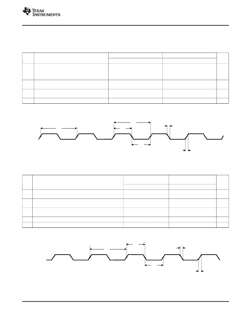
Figure 5-9. CLKIN Timing
Table 5-5. Switching Characteristics Over Recommended Operating Conditions for CLKOUT (1)
(2)
CV DD = 1.05 V
CV DD = 1.3 V
NO.
PARAMETER
V DDA_PLL = 1.3 V
MIN
MAX
V DDA_PLL = 1.3 V
MIN
MAX
UNIT
1
t c(CLKOUT)
Cycle time, CLKOUT
P
16.67 or
13.33
P
10 or 8.3
ns
2
3
4
5
t w(CLKOUTH)
t w(CLKOUTL)
t t(CLKOUTR)
t t(CLKOUTF)
Pulse duration, CLKOUT high
Pulse duration, CLKOUT low
Transition time (rise), CLKOUT
Transition time (fall), CLKOUT
0.466 *
t c(CLKOUT)
0.466 *
t c(CLKOUT)
5
5
0.466 *
t c(CLKOUT)
0.466 *
t c(CLKOUT)
5
5
ns
ns
ns
ns
(1)
(2)
The reference points for the rise and fall transitions are measured at V OL MAX and V OH MIN.
P = 1/SYSCLK clock frequency in nanoseconds (ns). For example, when SYSCLK frequency is 100 MHz, use P = 10 ns.
2
1
5
CLKOUT
3
4
Figure 5-10. CLKOUT Timing
Copyright ? 2010–2013, Texas Instruments Incorporated
Peripheral Information and Electrical Specifications
Product Folder Links: TMS320C5515
81
发布紧急采购,3分钟左右您将得到回复。
相关PDF资料
TMDXEXP1808L
KIT EXPERIMENTER FOR AM180X
TO263-3EV-VREG
BOARD EVAL TO220-3/TO263-3 VREG
TO263-5EV-VREG
EVAL BOARD VREG TO220-5/TO263-5
TOOLSTICK-EK
KIT TOOL EVAL SYS IN A USB STICK
TPS23757EVM
EVALUATION MODULE FOR TPS23757
TPS62230EVM-370
EVAL MODULE FOR TPS62230-370
TRAVELCUBE
SURGE SUP 1OUT W/RJ11 DIRECTPLUG
TRAVELER100BT
SURGE SUP 2OUT W/RJ11 DIRECTPLUG
相关代理商/技术参数
TMDXEVM5515
制造商:Texas Instruments 功能描述:TMS320C5515 DSP Evaluation Module
TMDXEVM642
制造商:Texas Instruments 功能描述:Tools Development kit For Use
TMDXEVM6424
功能描述:开发板和工具包 - TMS320 C6424 DSP Eval Mod RoHS:否 制造商:Texas Instruments 产品:Experimenter Kits 工具用于评估:F2802x 核心:TMS320 接口类型:UART, USB 工作电源电压:
TMDXEVM6446
制造商:Rochester Electronics LLC 功能描述:DAVINCI EVM BUNDLE W/O EMULATOR - Bulk 制造商:Texas Instruments 功能描述:DAVINCI EVM BUNDLE W/O EMULATOR - Bulk
TMDXEVM6446T
制造商:Texas Instruments 功能描述:DM6446 DIGITAL VIDEO EVALUATION MODULE - Boxed Product (Development Kits)
TMDXEVM6446TS
制造商:Texas Instruments 功能描述:DM6446 DIGITAL VIDEO EVALUATION MODULE - Trays
TMDXEVM6452
功能描述:开发板和工具包 - TMS320 C6452 EVM Evaluation Module RoHS:否 制造商:Texas Instruments 产品:Experimenter Kits 工具用于评估:F2802x 核心:TMS320 接口类型:UART, USB 工作电源电压:
TMDXEVM6455
功能描述:开发板和工具包 - TMS320 C6455 Evaluation Module RoHS:否 制造商:Texas Instruments 产品:Experimenter Kits 工具用于评估:F2802x 核心:TMS320 接口类型:UART, USB 工作电源电压:
